Large-area nanostructures with atomic precision
- Photo Info
- Download
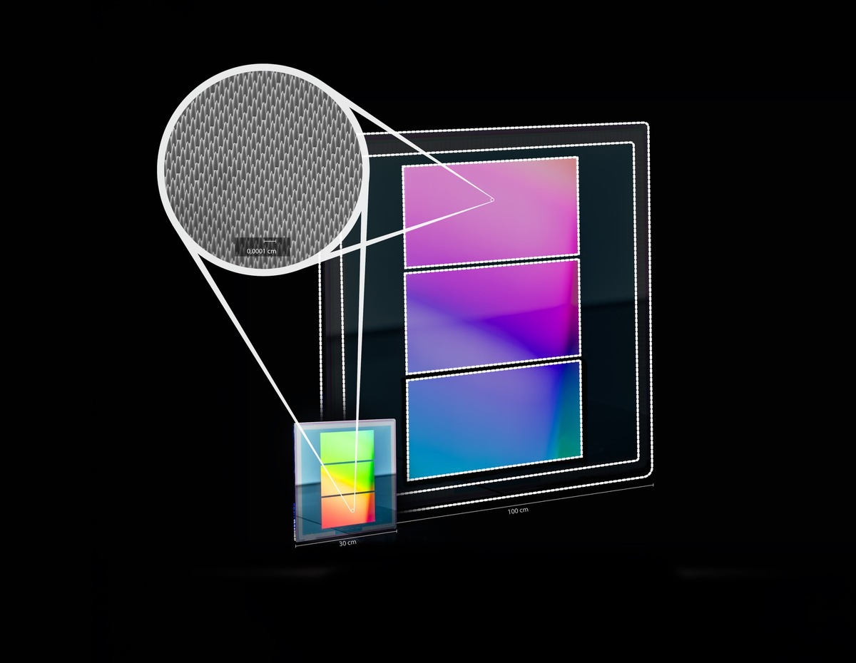
With conventional methods, high-precision nanostructures on photonic components can currently only be produced up to a size of 30 centimeters. Researchers in Thuringia are now working on the development of a new machine that will be able to create nanostructures spanning up to one square meter in the future—with a positioning accuracy smaller than an atom. The underlying research project, funded by the Deutsche Forschungsgemeinschaft (DFG, German Research Foundation) with four million euros, will launch with a kickoff event on May 6 in Erfurt as part of the Quantum Photonics trade fair.
Thuringian researchers aim to develop a new 3D nanolithography and nanomeasuring machine that will enable the processing and measurement of photonic components with dimensions of up to 1 × 1 × 0.2 meters. This is about three times larger than what is possible with current methods. Researchers from the Fraunhofer Institute for Applied Optics and Precision Engineering IOF in Jena, as well as the Institute of Applied Physics (IAP) at Friedrich Schiller University Jena and the Technical University of Ilmenau, have now begun the necessary development work as part of a project funded by DFG.
High-precision nanostructuring on a new scale
“The fact that there are machines for structuring large-area components is, at first glance, nothing unusual,” explains Prof. Uwe Zeitner, project leader at Fraunhofer IOF. “Many modern TV sets have displays that incorporate nanotechnology. But they are nowhere near as precise as we need them to be in various scientific applications. Scientific applications require high-precision nanostructuring. With conventional technologies, such structures can currently only be produced with the necessary precision on photonic components and parts with a size of up to approximately 30 centimeters. For many fields of future research—including fusion and gravitational wave research—we need optical components with significantly larger surfaces, such as nanostructured high-performance mirrors with a diameter of one meter that also offer the highest possible precision in light reflection.”
Target precision smaller than an atom
This precision—along with the scaling up in size—is the highlight of the planned machine: “We want to create nanostructures with a positioning accuracy across this surface of up to twenty picometers,” Zeitner continues. For comparison: One picometer corresponds to one trillionth of a meter. A picometer is thus about a hundred times smaller than the diameter of an atom.
“Our goal is to develop and build a state-of-the-art and globally unique machine that will enable us to manufacture new high-performance optical components at the limits of what is technically feasible,” says Zeitner. “To achieve this, we are imposing these specific accuracy requirements on the new machine. In addition to the aforementioned positioning accuracy, we are aiming for a maximum structuring deviation of less than ten nanometers on a three-dimensional surface spanning one square meter.”
Nanolithography from Jena, positioning and measurement technology from Ilmenau
To achieve these enormous geometric dimensions, a whole range of innovative approaches must be employed. “These are largely unique in their complexity and reflect the long-standing and comprehensive expertise of all partners involved,” explains Zeitner. Fraunhofer IOF and IAP in Jena are contributing highly advanced methods for 3D nanolithography to the development work, while the Technical University of Ilmenau is contributing its expertise in extremely precise nanopositioning and nanometrology.
Application in fusion and gravitational wave research
The new machine holds particular promise for the production of large-area photonic components for energy and fusion research, as well as for gravitational wave research. The Fraunhofer IOF is already conducting a wide range of research in both of these fields: for example, highly sensitive sensors were developed and manufactured at the institute for the planned Einstein Telescope, the most precise gravitational wave detector to date. Meanwhile, research is underway on highly reflective and robust coatings for laser fusion. This makes the planned machine and the prospective provision of additional high-performance photonic components particularly well-suited for the Thuringian researchers.
Machine to be operational at Fraunhofer IOF starting in 2032
In the first project phase, which is scheduled to last three years, an overall concept will now be developed. Based on this, key subsystems will be developed and built, and proof of the achievement of the specified parameters will be provided. The fully operational machine is expected to be available at Fraunhofer IOF in approximately six years.
The development work is being carried out as part of the DFG program “New Devices for Research.” The DFG is funding the project with approximately four million euros.
Kickoff at Quantum Photonics in Erfurt
As part of Quantum Photonics Erfurt, the trade fair for quantum technologies newly held in Thuringia’s state capital since 2025, the project partners will present the development project for the 3D nanolithography and nanomeasuring machine (3D-NLM machine for short) to the public for the first time. The joint kickoff event will take place on May 6 from 1:00 p.m. to 2:00 p.m. as part of the trade fair’s conference.
Interested trade fair visitors are cordially invited to attend.
Further Information - Nanostructuring: Selected Examples at Fraunhofer IOF
Nanostructures are extremely fine structures that specifically manipulate light by influencing its wavelength. Over the past twenty years, such structures have become a key tool for overcoming a wide range of technological challenges. Nanostructures play a central role, for example, in the manufacture of integrated electronic and photonic circuits, in measurement technology and sensor technology, and even in high-performance optics for Earth observation, space research, and basic research.
Research on ultra-fine nanostructures is a major focus of Fraunhofer IOF. In 2023, the institute produced a nanostructured metasurface measuring 30 centimeters—a record achievement. In addition, the institute has repeatedly contributed nanostructured and mission-critical components for international space missions such as Sentinel 4, Sentinel 5, and CO2M in recent years. Further application potentials are opening up in quantum technologies, specifically quantum computing, through the fabrication of photonic quantum chips.
Desiree Haak
Press & Public Relations | Teamlead Communication
Fraunhofer Institute for Applied Optics and Precision Engineering IOF
Albert-Einstein-Strasse 7, 07745 Jena, Germany
phone:  +49 3641 807 – 803
mobile: +49 151 22 17 99 11
 http://www.iof.fraunhofer.de